The SP2-Lab was established in Apr. 2020, with the launch of the KUAS Faculty of Engineering. Activities in the Lab focus on the characterization, circuit deployment and integration of wide-band-gap (WBG) semiconductor devices (silicon carbide, SiC; gallium nitride, GaN).
With the transition of WBG semiconductor devices from a research topic to industrial products about 10-15 years ago, the initial focus has been mainly on their deployment within estalished solutions as a drop-in replacement of silicon (Si) devices. In this framework, the capability of WBG to outperform Si in terms of efficiency and power density was amply demonstrated.
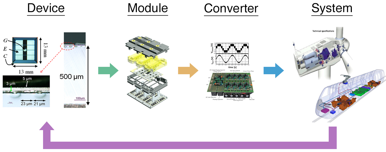
Today, the SP2-Lab activities focus on the development of WBG-bespoke solutions, both at topology and technology level. A holistic approach is pursued encompassing device, module, converter and system level analysis and synthesis to ensure well-matched and seamless integration of the functional and structural characteristics of all components.
Research focus areas
Research in the Lab is organised around three core thematic areas: circuits, devices and integration.
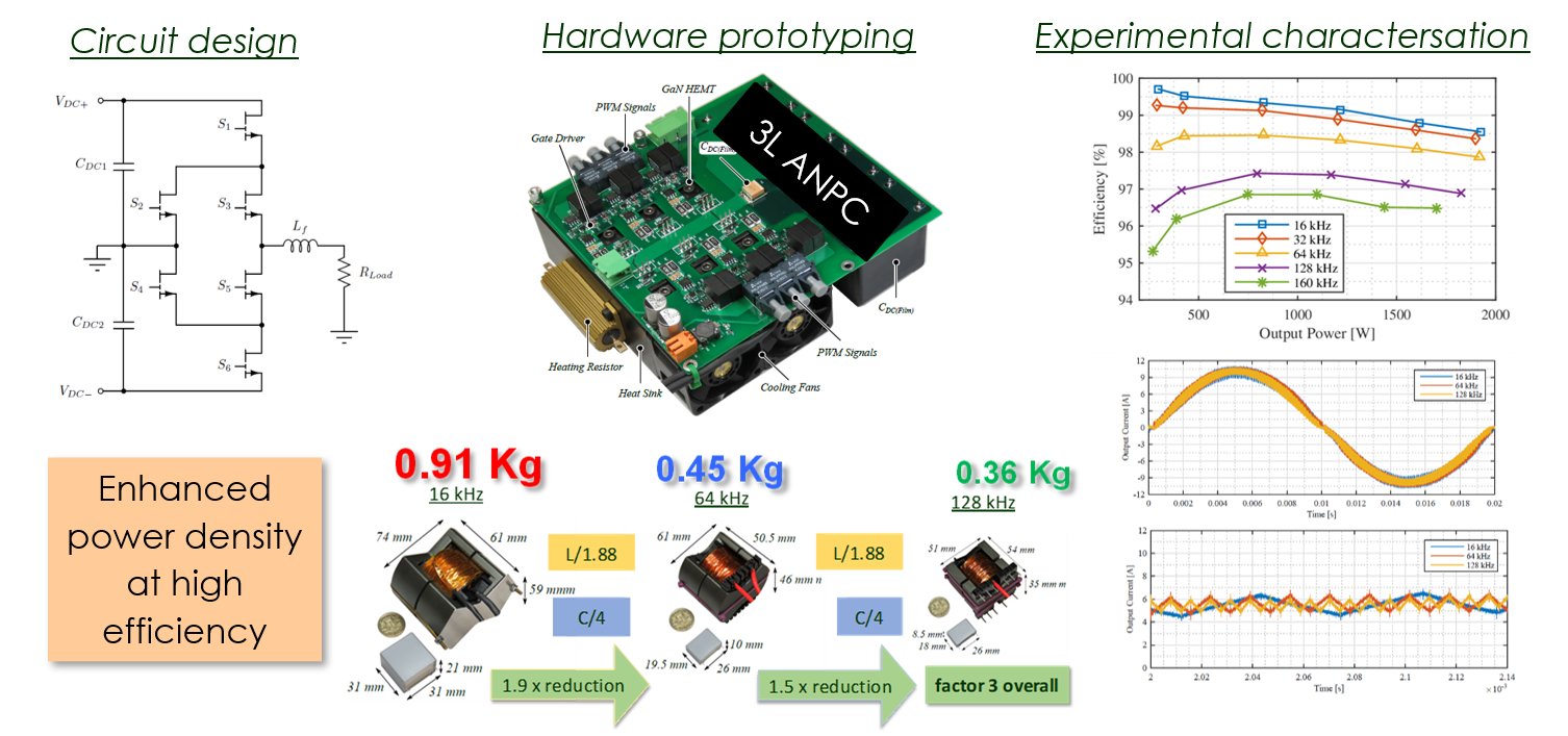
Circuits: activities in this domain focus on the development of innovative high-efficiency high-power-density multi-level, current source and Y-inverters, as well as DC-DC converters and innovative solutions for wireless power transfer applications. All activities include computer-aided design, hardware prototyping and extensive experimental demonstration, relying on state-of-the-art equipment and tools.
Devices
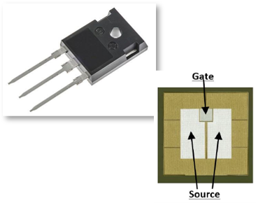
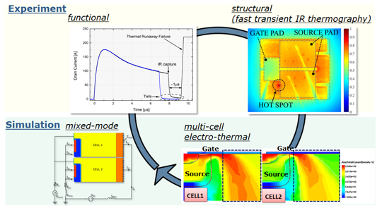
: work on devices encompasses both their functional electro-thermal and reliability characterisation as packaged units, as well as their structural characterisation in the form of bare dies (e.g., infrared termography, 3D x-ray tomography). By coupling the two areas of analysis, the device ultimate performance and robustness limits can be understood. Further, the iterative co-deployment of experimental and physical simulation methodologies enables the formulation of innvoative design options yielding progress beyond state-of-the-art.
Integration
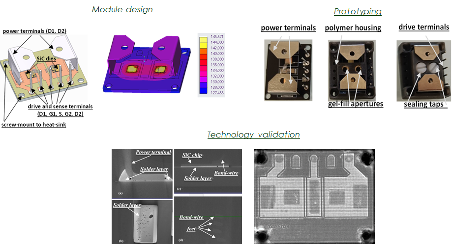
: integration is the key discipline to match form to function, technologies to topologies, and make the most of WBG semiconductor device characteristics. By developing custom packaging solutions, the electro-thermal, electro-magnetic and thermo-mechanical performance of the system can be greatly enhanced. Moreover, present efforts aim at counterbalancing the higher cost of WBG devices over Si ones by developing innovative cost-competitive alternatives to conventional ones.
Research projects and collaborations
2020-2023: JSPS Kakenhi Grant 20H02138 (Kiban "B") "Energy-efficient lightweight drives by multi-parametric machine-inverter co-design and split-mid-point modularization" (in collaboration with Prof. T. Nakamura - Kyoto University)
2020-2023: JSPS Kakenhi Grant 20H02151 (Kiban "B") "小容量電力伝送のデジタル化を実現するための基盤技術の構築" (in collaboration with Prof. T. Hikihara - Kyoto University)
2020-2021: Industrial sponsorship "High-frequency GaN-based non-inverting buck-boost
DC-DC converter for LED applications" (in collaboration with sponsor)
2021-2024: JSPS Kakenhi Grant 21H01311 (Kiban "B") "Development of reliable SiC MOSFET power modules" (in collaboration with Prof. T. Funaki - Osaka University)
2021-2024: KUAS Internal Sponsorship "Kameoka SiC EV" (in collaboration with Prof. T. Nakamura - Kyoto University and Prof. S. Domae - Nagamori Institute of Actuators)
The Lab has a number of ongoing collaborations and exchanges with other academic and industrial partners in Japan and overseas.
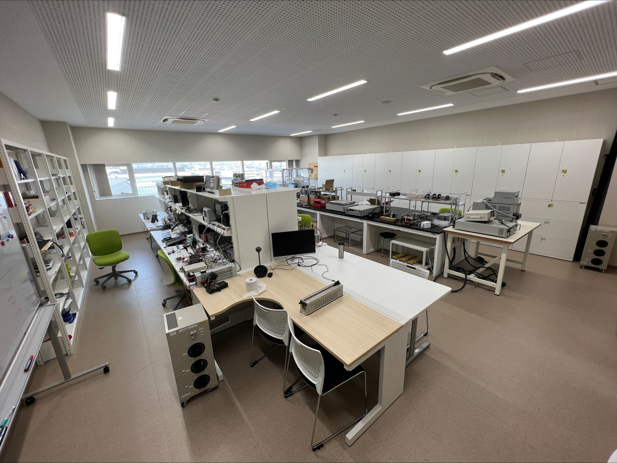
Facilities and equipment
The Lab has capacity for about 16 reserachers and enjoys beautiful views over the north-side Kyoto mountains (Daimonji).
It is equipped with and has access to :
- DC and AC power supplies (up to: 1.5 kV, 300 A and 20 kW testing capability);
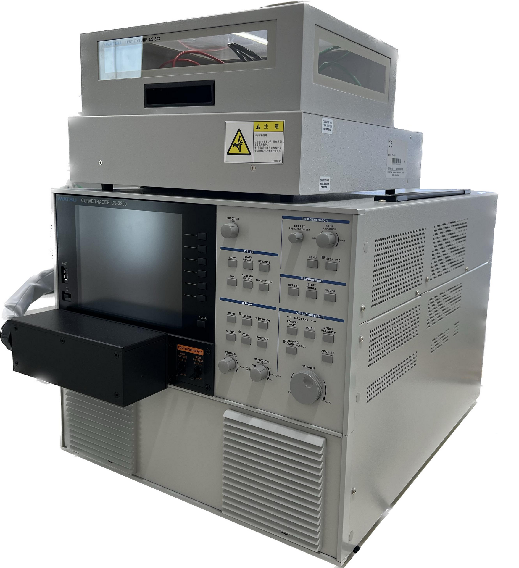
- 3 kV/400 A curve tracer
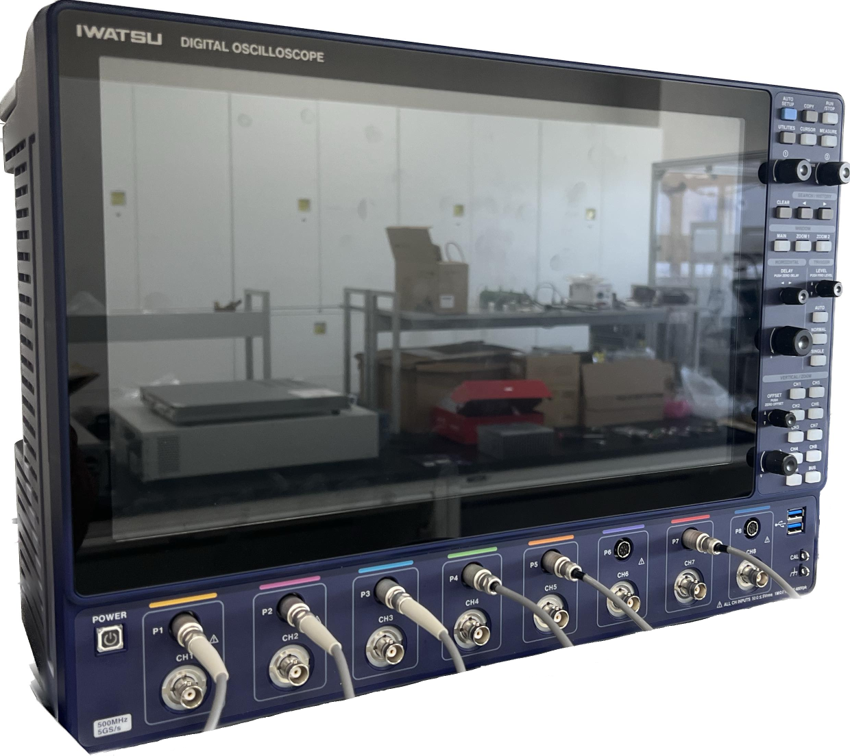
- broad-bandwidth oscilloscopes and voltage/current probes
- power, impedance and spectrum analyzers
- active loads and resistive load banks
- infrared thermal imaging capability
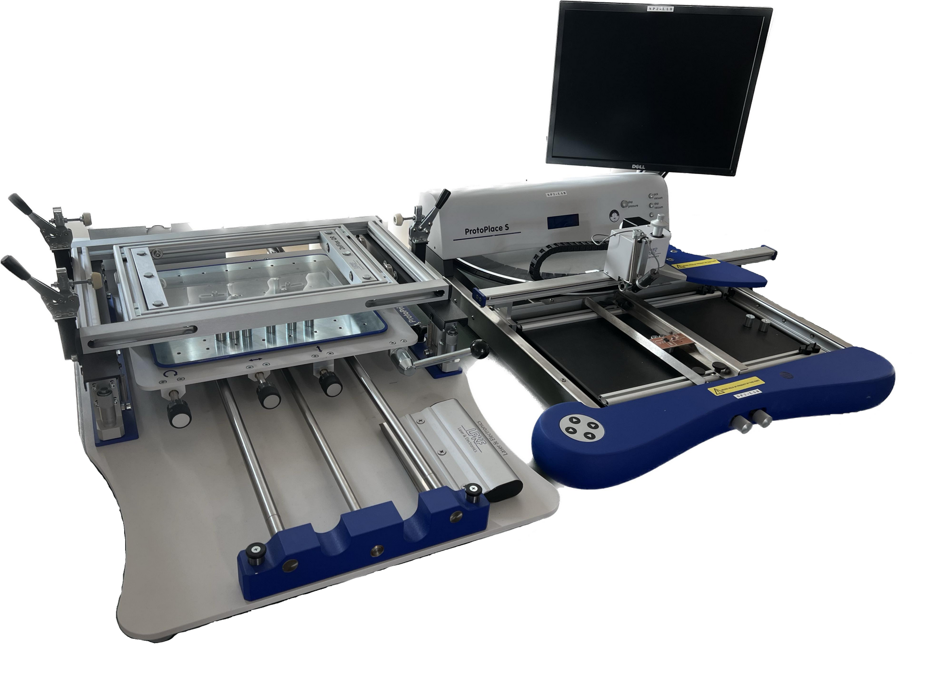
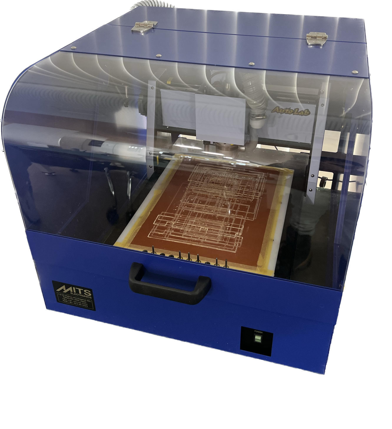
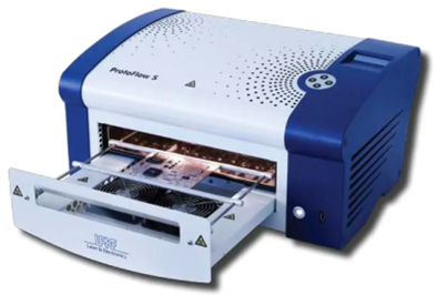
- 2-layer PCB prototyping, semi-automatic SMD device assembly, laser plotting, stencil printing and reflow oven
- control boxes (Imperix B-Box/B-Board, Labview/NI, Digilent)
- all-round T-CAD capability (OrCAD-Spice, PSIM, PLECS, Matlab-SIMULINK, Altium Designer; Sentaurus; CREO)
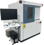
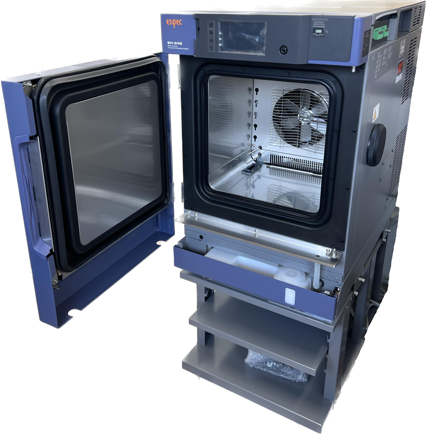
- thermal chambers and 3D X-ray tomography
The Lab members are involved in the delivery of the following courses:
Semiconductor Engineering: this is a 3rd year course (first semester) covering the fundamentals of semiconductor physics and technology, as well as the main power devices (e.g., pin and Schottky diodes, BJTs, power MOSFETs, IGBTs, Thyristors), their application and thermal management.
Power Electronics Engineering: this is a 3rd year course (second semester) covering the fundamentals of AC and DC power suply, pulse-width-modulation (PWM), non-isolated dc-dc converters, two-level single-phase and three-phase inverters, recitifiers and matrix converters. F
or the delivery, ample
use is made of simulation-based exercises using pSpice and Matlab-Simulink.
Mechatronics Laboratory (Energy): this is a 3rd year laboratory-based module focusing on electrical machines, power electronics and bateries. Students are expected to work 4.5 hrs/week over 15 weeks. The power electronics section involves mini-project focusing on the design and prototype developmnt and test of a re-confiugurable 4-switch power converter architecture, which can be used as a rectifier, a step-up/down dc-dc converter and a single-phase inverter, using both bipolar and unipolar modulation schemes. Students work in groups and are expected to take the lead on the simulation, prototype assembly, testing and techncial reporting.
Enabling Technologies of Solid-State Power Conversion: this is a post-graduate level course avaiable to MSc and PhD students alike. The course deals with the fundamentals of semiconductor devices, their packaging, applciation, thermal management and reliability.
Computer-Aided-Design of Power Semiconductor Devices and Modules: this is
a post-graduate level course available to MSc and PhD students alike. It deals with some of the fundamental euqations of engineering (e.g., diffusion, Poisson/Laplace) and their numerical solution in the presence of various initial and boundary conditions. The course includes a substantial part of practical computer exercises using Matlab and CREO.
Prof. Castellazzi also teaches part-time at Kyoto University (Power Electronics) and Tokyo Metropolitan University (Trends and Challenges of Modern Power Conversion)
created with
Best HTML editor .